Design-Induced Latency Variation in Modern DRAM Chips: Characterization, Analysis, and Latency Reduction Mechanisms

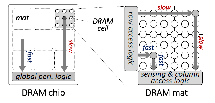
Variation has been shown to exist across the cells within a modern DRAM chip. Prior work has studied and exploited several forms of variation, such as manufacturing-process- or temperature-induced variation. We empirically demonstrate a new form of variation that exists within a real DRAM chip, induced by the design and placement of different components in the DRAM chip: different regions in DRAM, based on their relative distances from the peripheral structures, require different minimum access latencies for reliable operation. In particular, we show that in most real DRAM chips, cells closer to the peripheral structures can be accessed much faster than cells that are farther. We call this phenomenon design-induced variation in DRAM. Our goals are to i) understand design-induced variation that exists in real, state-of-the-art DRAM chips, ii) exploit it to develop low-cost mechanisms that can dynamically find and use the lowest latency at which to operate a DRAM chip reliably, and, thus, iii) improve overall system performance while ensuring reliable system operation. To this end, we first experimentally demonstrate and analyze designed-induced variation in modern DRAM devices by testing and characterizing 96 DIMMs (768 DRAM chips). Our characterization identifies DRAM regions that are vulnerable to errors, if operated at lower latency, and finds consistency in their locations across a given DRAM chip generation, due to design-induced variation. Based on our extensive experimental analysis, we develop two mechanisms that reliably reduce DRAM latency. First, DIVA Profiling uses runtime profiling to dynamically identify the lowest DRAM latency that does not introduce failures. DIVA Profiling exploits design-induced variation and periodically profiles only the vulnerable regions to determine the lowest DRAM latency at low cost. It is the first mechanism to dynamically determine the lowest latency that can be used to operate DRAM reliably. DIVA Profiling reduces the latency of read/write requests by 35.1%/57.8%, respectively, at 55℃. Our second mechanism, DIVA Shuffling, shuffles data such that values stored in vulnerable regions are mapped to multiple error-correcting code (ECC) codewords. As a result, DIVA Shuffling can correct 26% more multi-bit errors than conventional ECC. Combined together, our two mechanisms reduce read/write latency by 40.0%/60.5%, which translates to an overall system performance improvement of 14.7%/13.7%/13.8% (in 2-/4-/8-core systems) across a variety of workloads, while ensuring reliable operation.
Publication Date
Research Area
External Links
Uploaded Files
Copyright
Copyright by the Association for Computing Machinery, Inc. Permission to make digital or hard copies of part or all of this work for personal or classroom use is granted without fee provided that copies are not made or distributed for profit or commercial advantage and that copies bear this notice and the full citation on the first page. Copyrights for components of this work owned by others than ACM must be honored. Abstracting with credit is permitted. To copy otherwise, to republish, to post on servers, or to redistribute to lists, requires prior specific permission and/or a fee. Request permissions from Publications Dept, ACM Inc., fax +1 (212) 869-0481, or permissions@acm.org. The definitive version of this paper can be found at ACM's Digital Library http://www.acm.org/dl/.
