A 0.54 pJ/b 20 Gb/s Ground-Referenced Single-Ended Short-Reach Serial Link in 28 nm CMOS for Advanced Packaging Applications
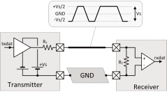
High-speed signaling over high density interconnect on organic package substrates or silicon interposers offers an attractive solution to the off-chip bandwidth limitation problem faced in modern digital systems. In this paper, we describe a signaling system co-designed with the interconnect to take advantage of the characteristics of this environment to enable a high-speed, low area, and low-power die to die link. Ground-Referenced Signaling (GRS) is a single-ended signaling system that eliminates the problems traditionally associated with single-ended design by using the ground plane as the reference and signaling above and below ground. This design employs a novel charge pump driver that additionally eliminates the issue of simultaneous switching noise with data independent current consumption. Silicon measurements from a test chip implementing two 16-lane links, with forwarded clocks, in a standard 28nm process demonstrate 20Gb/s operation at 0.54pJ/bit over 4.5mm organic substrate channels at a nominal 0.9V power supply voltage. Timing margins at the receiver are >0.3UI at a BER of <10^-12 . We estimate BER < 10^-25 at the eye center.
Publication Date
Published in
Research Area
Copyright
This material is posted here with permission of the IEEE. Internal or personal use of this material is permitted. However, permission to reprint/republish this material for advertising or promotional purposes or for creating new collective works for resale or redistribution must be obtained from the IEEE by writing to pubs-permissions@ieee.org.