A 1.17-pJ/b, 25-Gb/s/pin Ground-Referenced Single-Ended Serial Link for Off- and On-Package Communication Using a Process- and Temperature-Adaptive Voltage Regulator
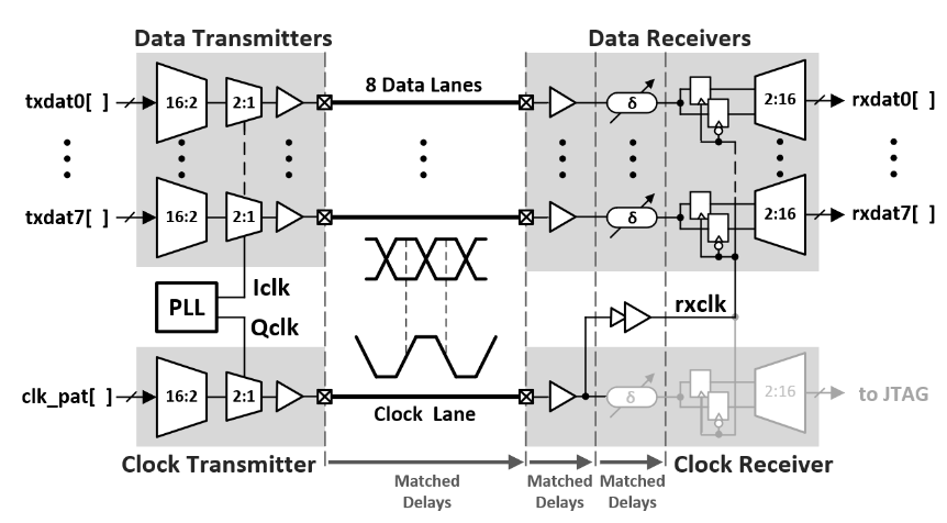
This paper describes a short-reach serial link to connect chips mounted on the same package or on neighboring packages on a printed circuit board (PCB). The link employs an energy-efficient, single-ended ground-referenced signaling scheme. Implemented in 16-nm FinFET CMOS technology, the link operates at a data rate of 25 Gb/s/pin with 1.17-pJ/bit energy efficiency and uses a simple but robust matched-delay clock forwarding scheme that cancels most sources of jitter. The modest frequency-dependent attenuation of short-reach links is compensated using an analog equalizer in the transmitter. The receiver includes active-inductor peaking in the input amplifier to improve overall receiver frequency response. The link employs a novel power supply regulation scheme at both ends that uses a PLL ring-oscillator supply voltage as a reference to flatten circuit speed and reduce power consumption variation across PVT. The link can be calibrated once at an arbitrary voltage and temperature, then track VT variation without the need for periodic re-calibration. The link operates over a 10-mm-long on-package channel with −4 dB of attenuation with 0.77-UI eye opening at bit-error rate (BER) of 10−15. A package-to-package link with 54 mm of PCB and 26 mm of on-package trace with −8.5 dB of loss at Nyquist operates with 0.42 UI of eye opening at BER of 10−15. Overall link die area is 686 μm × 565 μm with the transceiver circuitry taking up 20% of the area. The transceiver’s on-chip regulator is supplied from an off-chip 950-mV supply, while the support logic operates on a separate 850-mV supply.
Publication Date
Published in
Research Area
Uploaded Files
Copyright
This material is posted here with permission of the IEEE. Internal or personal use of this material is permitted. However, permission to reprint/republish this material for advertising or promotional purposes or for creating new collective works for resale or redistribution must be obtained from the IEEE by writing to pubs-permissions@ieee.org.